


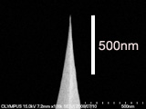
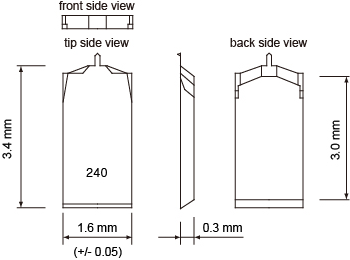
AFM探针 扫描探针 OLTESPA OMCL-AC240TS


OMCL-AC240TS-R3
OMCL-AC240TS-,
标准型(Standard Silicon Cantilever)
Tip Schematic
| Geometry: | Visible Apex |
| Tip Height (h): | 9 - 19µm |
| Front Angle (FA): | 0 ± 1º |
| Back Angle (BA): | 35 ±1 º |
| Side Angle (SA): | 18 ±1 º |
| Tip Radius (Nom): | 7 nm |
| Tip Radius (Max): | 10 nm |
| Tip SetBack (TSB)(Nom): | 0 µm |
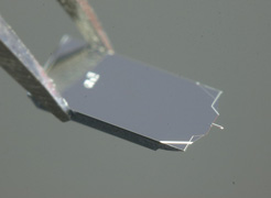
designed for AC mode AFM in air to observe topography and viscoelasticity of soft samples.
Outstanding features
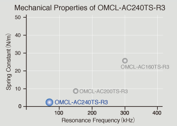
- 1. Small spring constant for the measurements of soft samples
- 2. Measuring surface potential with low resistivity silicon
- 3. Ideally point terminated probe
- 4. Acclaimed ‘TipView’ structure
- 5. Reflex side aluminum coating
- 6. Ease in chip handling: ‘New concept chip’
- 7. Packaging: Pre-separated chips
More about New OMCL-AC240 series
1. Small spring constant for the measurements of soft samples
Spring constant of 2 N/m(Typ.) is the smallest in our silicon cantilevers for AC mode, suitable for observing surface topography and viscoelasticity of soft samples.
2. Measuring surface potential with low resistivity silicon
Cantilever base material employs N-type doped silicon with a surface resistance of 0.01-0.02 Ω · cm (1/200th the surface resistance of our other base materials). This can be achieved to use for measuring surface potential and other applications.
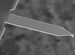
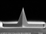
3. Ideally point terminated probe
The apex of the tetrahedral probe is ideally point terminated.
The tetrahedral probe shows good symmetry viewed from the front. Considering the geometric feature, choose the fast scan (X) direction. Check Scan line profile and enlarged view of the tip apex.
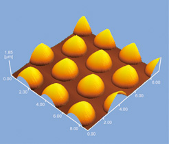
Patterned Sapphire Substrate 9 µm x 9 µm
Sample, courtesy of MAXIS, Korea
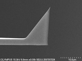
4. Acclaimed ‘TipView’ structure
The probe can be easily positioned at the exact point of your interest due to ‘TipView’ structure.
The probe is located at the exact end of the cantilever so that the probe apex is not obscured during optical observations.
5. Reflex side aluminum coating
Thin aluminum film with the thickness of 100 nm is coated on the cantilever for reflecting light from the deflection sensor in the AFM equipment. High reflex for high S/N sensing can be expected.
6. Ease in chip handling: ‘New concept chip’
The ideally vertical side-walls of the chip make tweezing easy and eliminate problems with chipping and debris.
 3D-AFM 显微照片及其相应的 ( a ) Ni-P、Ni-P-TiC 复合涂层的表面粗糙度曲线( b ) 0.5 g L -1 , ( c ) 1.0 g L -1 , ( d ) 1.5 g L -1和( e ) 2.0g L -1 TiC颗粒。
 含不同浓度 TiC 颗粒的 Ni-P 和 Ni-P-TiC 复合涂层的纳米压痕结果;( a ) 加载/卸载轮廓和 ( b ) 硬度。---OMCL-AC240TS-R3

8 nm 不同聚合物共混膜的 AFM 图像。
第一列是原始聚合物共混膜在用环己烷洗涤之前的 AFM 图像。为了去除共混膜中的PS,共混膜用环己烷洗涤。第二列显示了聚合物共混膜经环己烷洗涤后的 AFM 图像。第三列是沿着第一列和第二列中的线(灰线)的截面图。( a – c ), ( d–f ) 和 ( g – i ) 薄膜分别为 S20/M80、S50/M50 和 S80/M20。
特别提示:
近期市场出现不良销售代理商以OPUS的探针冒充Olympus的针尖,此行为不仅造成市场混乱,更给科研工作者带来了严重的实验数据及过程造成了无法弥补的结果,希望各位用户从正规渠道购买,如您发现有任何问题,欢迎来电咨询了解!
自2014年始北京创美伟业科技公司的探针业务均由上海分公司上海寰太电子科技有限公司/上海展悦电子科技有限公司承办,请给各位新老客户谅解!我公司是Olympus的大陆唯一总代,更有Olympus日本工程师实时在线支持,免您后顾之忧!
年度特惠活动正在进行中,欢迎各实验室/课题组来电咨询了解,18017933200(微信同号)郑小姐
秉持【诚信】,【创新】,【速效】的原则,至今已成为中国及香港地区,专业之系统之代理商。为了提供大家更高品质的产品及服务,我们将延续诚信的原则,热忱的态度,带给大家更高品质,更大众化,更丰富的专业产品。
地址:上海市闸北区汉中路汉中广场6F 电话:021-31683680 E-mail: sec.sh@biolab.com.cn
| 单位名称: |
|
详细地址:
上海市闸北区汉中路158号汉中广场6F
|
|
qq:
1597314722
|
|
联系电话:
021-31683680
|
| Email: |
